Overview
This webpage describes a well-developed optical sensor technolgy based on Bloch Surface Wave (BSW) resonance. I have been active in the development of this technology since the late 1980's and I hold 5 patents related to BSW applications. The goal of the web page is two-fold:
- Provide an introduction to the nature and applications of BSW phenomena for interested science and engineering researchers.
- Seek companies interested in licensing my patents and developing this promising sensing technology, as described in the Business Case for BSW Sensors section below.
I would be happy to respond to any technical research or business questions prompted by the material in this web page; my contact information is available below.
BSW Technology Basics
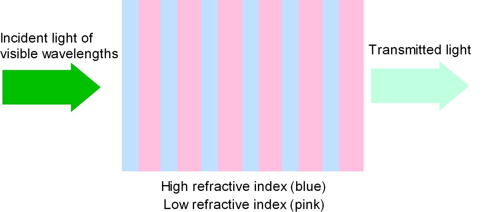
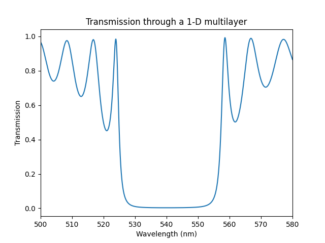
A BSW is a form of light (electromagnetic wave) that is confined to travel along the surface of a material that exhibits a photonic band gap. A photonic band gap (PBG) material is a periodic composite that possesses a frequency interval over which the propagation of light is strongly forbidden due to the coherent effects of scatttering and interference. Although there has been a wealth of research in the design of materials that are periodic in two- and three-dimensions, the simplest PBG material, and most amenable to manufacture, is periodic in only one dimension. Such materials consist of multiplayer structures composed of alternating layers of high and low refractive index materials. The figure below shows a sketch of a multilayer and a plot of the wavelength dependent transmission at normal incidence. The interference due to multiple refelections at the multilayer boundaries leads to a forbidden transmission region between 530 and 550 nm. BSWs can only exist within this forbidden transmission region. The mul;tilayer in this example consists of 10 TiO2/SiO2 bilayers with thicknesses 121 nm and 188 nm and refractive indices of 2.2 and 1.46 respectively.
In order to convert light in free space (such as a laser beam) into a BSW at the surface of a PBG multilayer some conditions must be met. First, the periodic multilayer must exhibit a PBG at the wavelength and incident angle of the incident light. Second, the multilayer must be truncated with a "defect" layer that breaks the regular periodicity of the multilayer with a last layer with a thickness that is either larger or smaller than the corresponding material in the periodic multilayer. Third, BSWs are non-radiative which means that they have a shorter wavelength at a given frequency than regular light at the same frequency in air. In practice this condition restricts the direct generation or decay or BSWs. Shining a laser in the surface of a multilayer structure that meets the first two criteria for supporting BSWs cannot result in coupling of light to the BSW because of the wavelength mismatch.
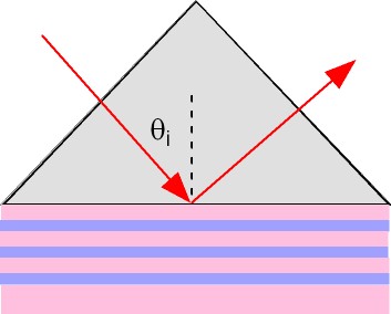
This phase matching restriction can be overcome with a prism coupling configuration. The figure below shows a schematic outlay of a prism coupling configuration. Note that the multilayer (greatly exaggerated for clarity) has a a last defect layer that is thicker than the other corresponding layers.
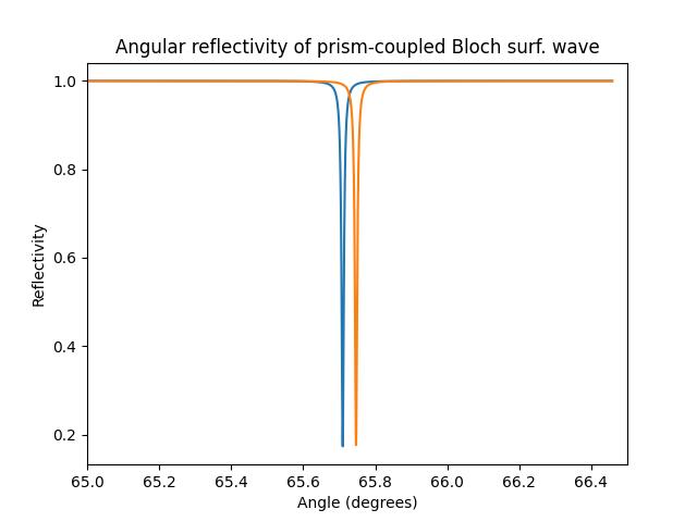
To generate BSWs light is incident through the prism. At angles greater than that for total internal reflection, the evanescent light is able to resonantly generate BSWs at the outer surface ofthe multilayer. Generation of BSWs only occurs at narrow angular range at which the parallel component of the incident light matches that of the BSW. The coupling of light to BSWs can be inferred by measuring the reflectivity. At the angle at which coupling to BSws occurs there is a sharp drop in the reflected intensity because the incident light is chenneled over to a BSW at the surface of the multilayer. A theoretical plot of reflectivity versus angle. is shown in the figure. The angular width of the reflectivity dip is about 0.01 degrees. The sensitivity of the angular position of the reflectivity minimum to changes at the outer surface of the multilayer is the basis of making a sensor. A change in refractive index or dielectric loading at the outer surface of the multilayer leads to a shift in the coupling angle. Dieletric loading can be realized by coating the multilayer with an antibody. Subsequent exposure to a solution containing the antigen will cause a small change in the conditions at the surface causing the reflectivity minimum to shift. In the figure above the reflectivity curve in blue is the bare multilayer. The orange curve is the reflectivity with a 2 nm thick layer representing biomolecule attachment by some form of antibody-antigen or DNA-probe reaction.
Bloch surface waves are often compared to surface plasmons. The two surface electromagnetic waves have some similarities; however, the use of surface plasmons sensors is a well established technology in the sensor marketplace. By far the largest company in surface plasmon sensing is Biacore which was for many years a part of GE Healthcare but as of 2020 has been spun off as Cytiva. Surface plasmons, like BSWs, are non-radiative surface electromagnetic waves which requires a prism coupling configuration. Surface plasmons are generated at the surface of metal films--for sensing the metal chosen is typically gold. Because of the intrinsic loss experienced by light in metals, the surface plasmon resonance is typically two orders of magnitude broader than the BSW resonance. More details on the relative merits of surface plasmons and BSWs for sensing is given in the Business case section below.
Business Case for BSW Sensors
A goal of this web document is to find a company willing to bring a BSW sensor to market taking advantage of my experience and my portfolio of patents on BSW phenomena. As this section outlines, BSW sensors represent a strongly competitive technology to surface plasmon sensors both in terms of performance and cost. Here I oputline the range of applications for BSW sensors and explain why BSW sensors offer some significant advantages over surface plasmon sensors.
Surface plasmon sensors are well-established and widely used in the chemical, pharmaceutical, and biotech industries. Both BSW and surface plasmon sensors act by measuring the change in resonance conditions due to small changes in the refractive index conditions at the surface of the sensor. The basic method of targeted sensing is to immobilize one moloecule of a binding pair (such as an antibody-antigen reaction) on the sensor surface. As the complementary target molecule is introduced, typically in a flow cell, the binding at the sensor surface is measured by the change in either coupling angle or wavelength of the resonance. Resonance sensors of this type give both yes/no answers as to the presence of a target molecule, but also by monitoring the changing resonance conditions as a function of time, the reaction rate dynamics.
What are the relative advantages of the BSW sensor compared to the surface plasmon sensor?
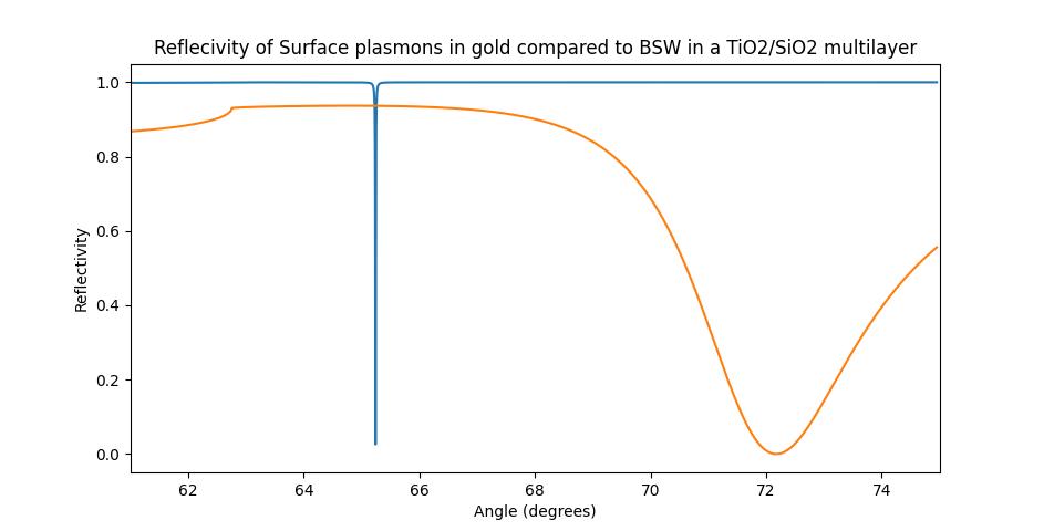
- BSW resonance is much narrower than surface plasmon resonance which means that the BSW system exhibits higher sensitivity than surface plasmon sensors. The difference in the sharpness of the resonances can be seen in the following reflectivity plot
which shows the BSW resonance (blue line) compared to that of gold (orange line) at the same wavelength.
- BSW sensors can be designed to work at essentially any wavelength in the infrared through the visible via the design of a suitable multilayer. In contrast surface plasmons in gold are restricted by the inherent dielectric properties of gold to wavelengths in the red and infrared parts of the optical spectrum.
- BSWs can be generated by light of either p- or s-polarization. Surface plasmons can only be excited by p-polarized light.
- Immobilization chemistry is required to attach target molecules to the sensor chip surface. Because the last layer of PBG multilayers is typically SiO2 (glass), the immobilization chemistry techniques are well established and understood. In contrast, surface plasmon sensors require binding molecules to gold. In addition to being more difficult chemically, many of the techniques are still covered by patents.
- The multilayer sensor chips are easy and inexpensive to manufacture using thin film deposition methods that are standard in the optics industry. One of my patents is for the sensor multilayer itself.
- The cost of a simple BSW sensor is much less than a surface plasmon sensor. As described in this paper, a simple flow cell sensor platform with 3D printed parts can be made for less than $250.
Sensor Configurations
BSW sensors have been demonstrated in a wide variety of configurations. The key factor is a system that monitors the change in the refractive index at the sensor chip surface. For prism coupled BSW sensors there are two basic configurations.
- Fixed incident wavelength and measure the reflectivity as a function of incident angle.
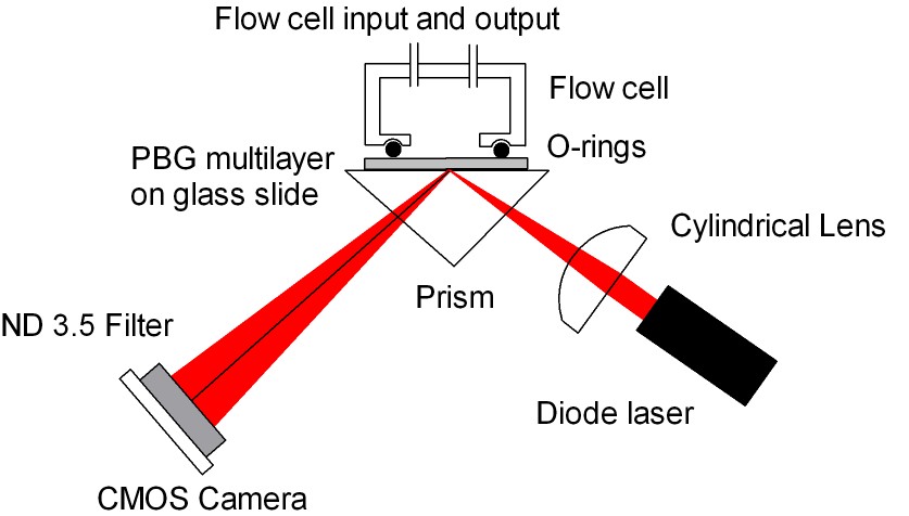
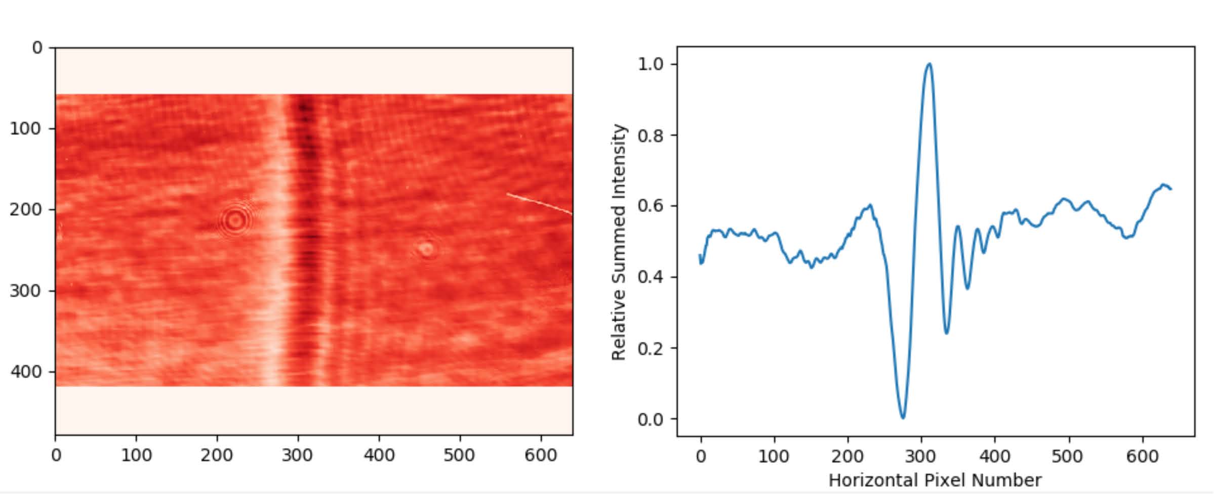
Fixed frequency means that a single wavelength laser source is used in a prism configuration as shown in the left panel of the figure below. The laser light is focused by a lens through the prism onto the sensor chip. Focusing creates a sperad of angles of incident light, only one angle of which will couple to the BSW while all off resonance light will be completely reflected. The reflected light is captured by a CMOS camera resulting in an image as shown in the middle panel of the figure. Summing the column of pixel data and plotting gives the rightmost plot. The change in pixel position of the reflectivity minimum with refractive index at the sensor chip surface is how sensing is accomplished.
- Fixed angle of incidence and measure the reflectivity as a function of wavelength.
- Microarray scanning sensor
A complete description of the laser based BSW sensor is given by the following reference.
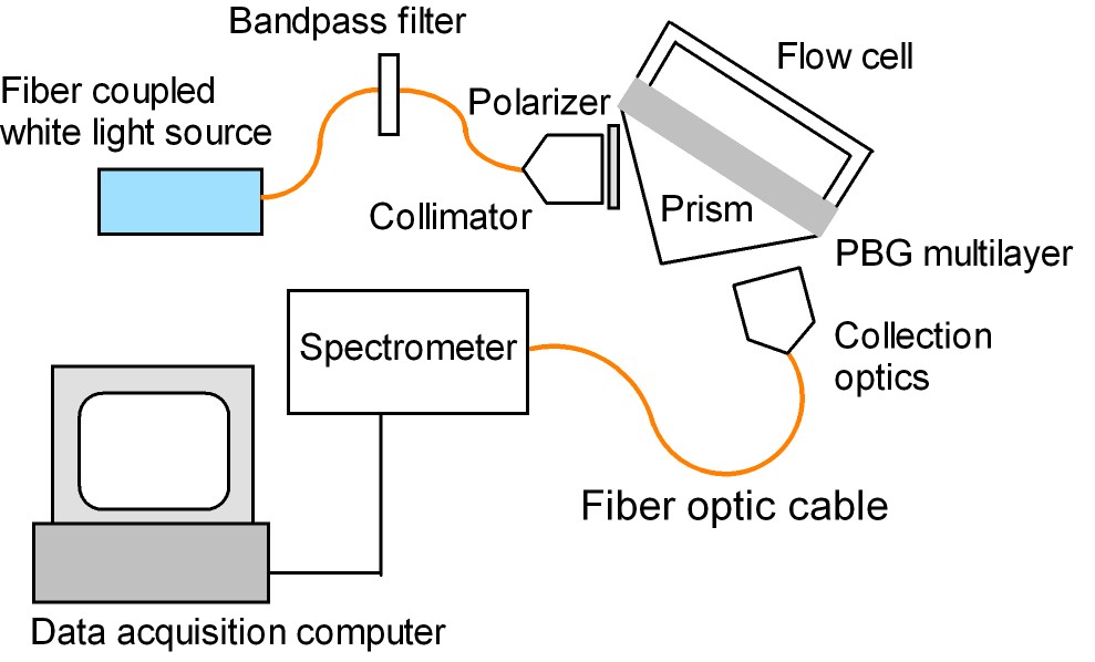
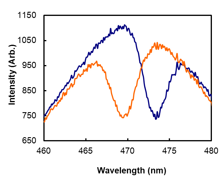
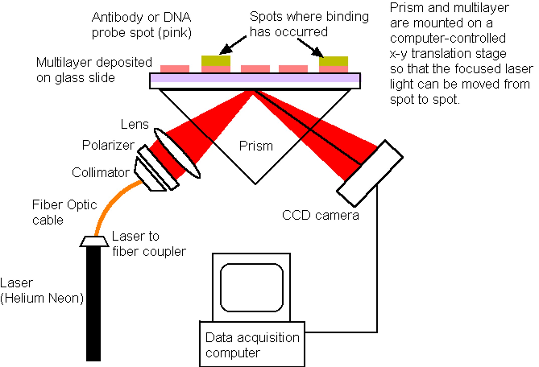
In this configuration a broad range of wavelengths is coupled to a single mode fiber optic and then collimated such that it forms a parallel beam incident on the sensor chip at an single fixed angle of incidnece. The reflected light is captured and fed to a small spectrometer. At the fixed angle of incidence, only a single narrow wavelength band will couple to the BSW with the remainder being reflected. This condition results in a reflectivity dip as a function of wavelength. The left panel of the figure below shows a schematic of the experimental layout. The right panel shows the spectral dip before and after explosure to a binding reaction. In this case the reaction is influenza DNA binding to a probe moelcule immobilized on the sensor surface.
A complete description of the laser based BSW sensor is given by the following reference.
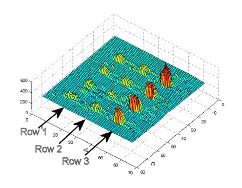
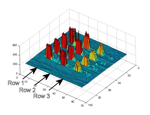
The previous two configurations used a flow cell configuration to monitor affinity binding reactions. An alternate configuration uses a fixed wavelength configuration but scans the focused laser spot across the surface of the sensor chip on which a microarray has been immobilized. Microarrays are a commonly used biotechnology technique and typically use fluorescent labels to determine when binding has occured. The use of the BSW sensor is a "label-free" technique that removes the need for fluorescence. The left figure in the panel below shows the experimental arrangement. The center and right panels show scans of a microarray of 12 spots in 3 rows of 4 spots. Rows 1 and 2 are spots of Bovine Serum Albumin (BSA) each 265 microns in diameter, whereas Row 3 is IgG. The center plot in the figure is a BSW scan of the array before exposure to anti-BSA. The BSA spots show a smaller shift (the bumps are “shorter”) than the IgG spots, as expected based on the relative size of the two entities. After exposure to anti-BSA, Rows 1 and 2 show a much larger angular shift because of the binding of BSA and anti-BSA. The IgG row is unaffected.
A complete description of the laser based BSW sensor is given by the following reference.
Bloch Surface Wave Patent Portfolio
I hold five patents on technology based on BSW phenomena. Three of the patents concern sensor configurations and the underlying design of the multilayer BSW sensor chip. The other two patents concern the use of BSWs for photonic circuits. A link to the text of each BSW patent is given below.
Bloch surface wave demo kit
I was one of the pioneers in the generation of Bloch surface waves in multilayers using a prism coupling arrangement. The ability to make a simple flow cell BSW sensor using 3D printed parts, cheap diode lasers, and simple optical components was demonstrated by my colleagues and me here . I am in the proceess of making the components available for purchase--particularly the multilayer optical chips which are the only components not readily available. This is a work in progress, but I would like to know if you are potentially interested. Please email me at the adress in the Contact section.
Contact
Phone: 615-838-7301
Email: bill@robertsonscience.com
Address: 1310 Roberts Road, Goodlettsville, TN, USA